

TL;DR #
Adding a graphite thermal interface layer (horizontal thermal conductivity 1600 W/m·K, thickness 0.03 mm) to a lamination-packaged COB LED module reduces operating junction temperature from 63.50 °C to 49.28 °C — a 14.22 °C reduction under 900 mA constant-current drive in 25 °C water. For buyers specifying underwater or high-humidity LED modules, thermal interface material selection is not a secondary consideration — it is the primary differentiator between a module that lasts and one that degrades. Before issuing any RFQ for sealed COB LED assemblies, require junction temperature test data under rated operating conditions, not just IP rating certificates.
Overview #
Most procurement teams evaluating sealed COB LED modules focus on IP rating and lumen output — and largely ignore the thermal interface stack. That is a costly oversight. Laboratory testing conducted at a university-affiliated optoelectronics research institute, using controlled constant-current drive conditions and forward voltage junction temperature measurement across multiple module configurations, shows conclusively that the choice of thermal conductive layer inside a laminated COB LED assembly determines operating junction temperature far more than encapsulation geometry alone.
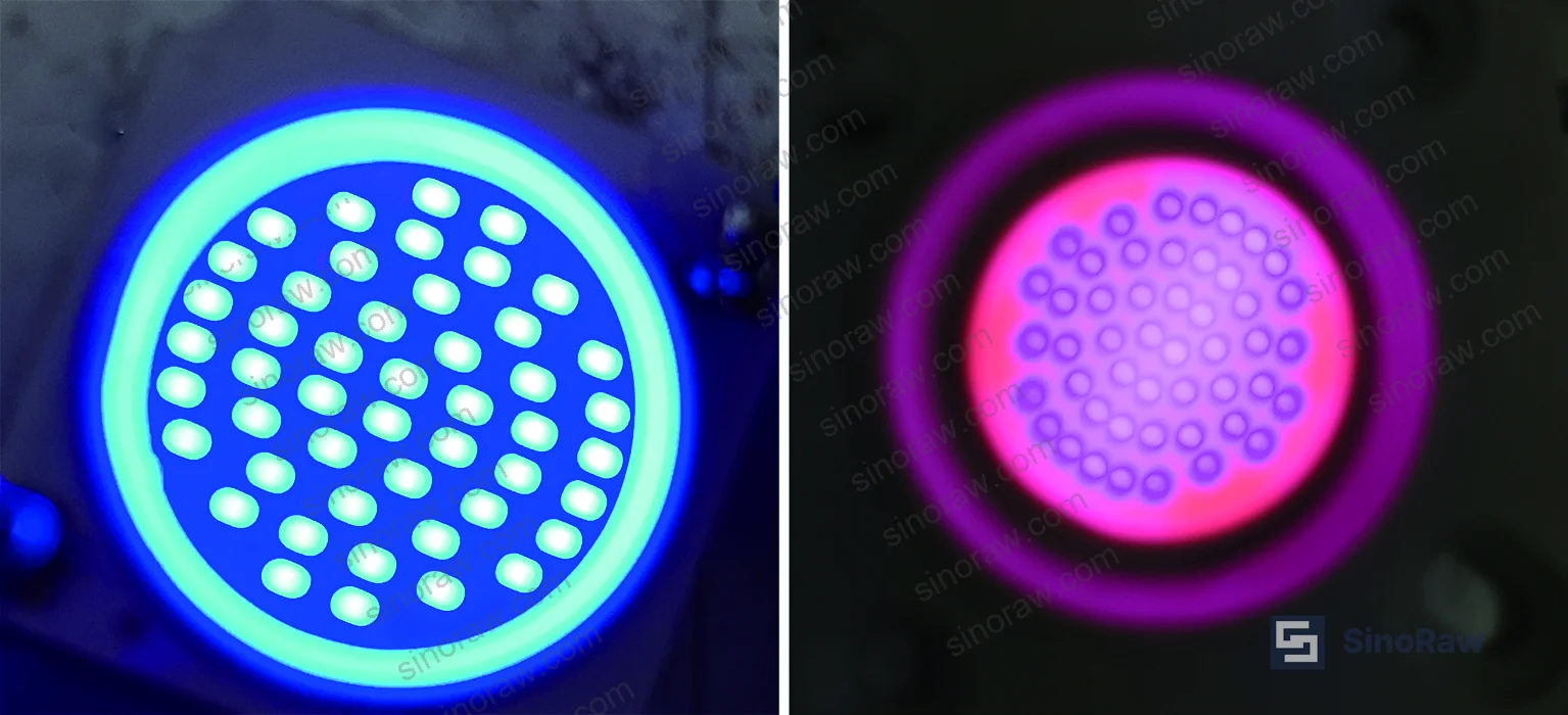
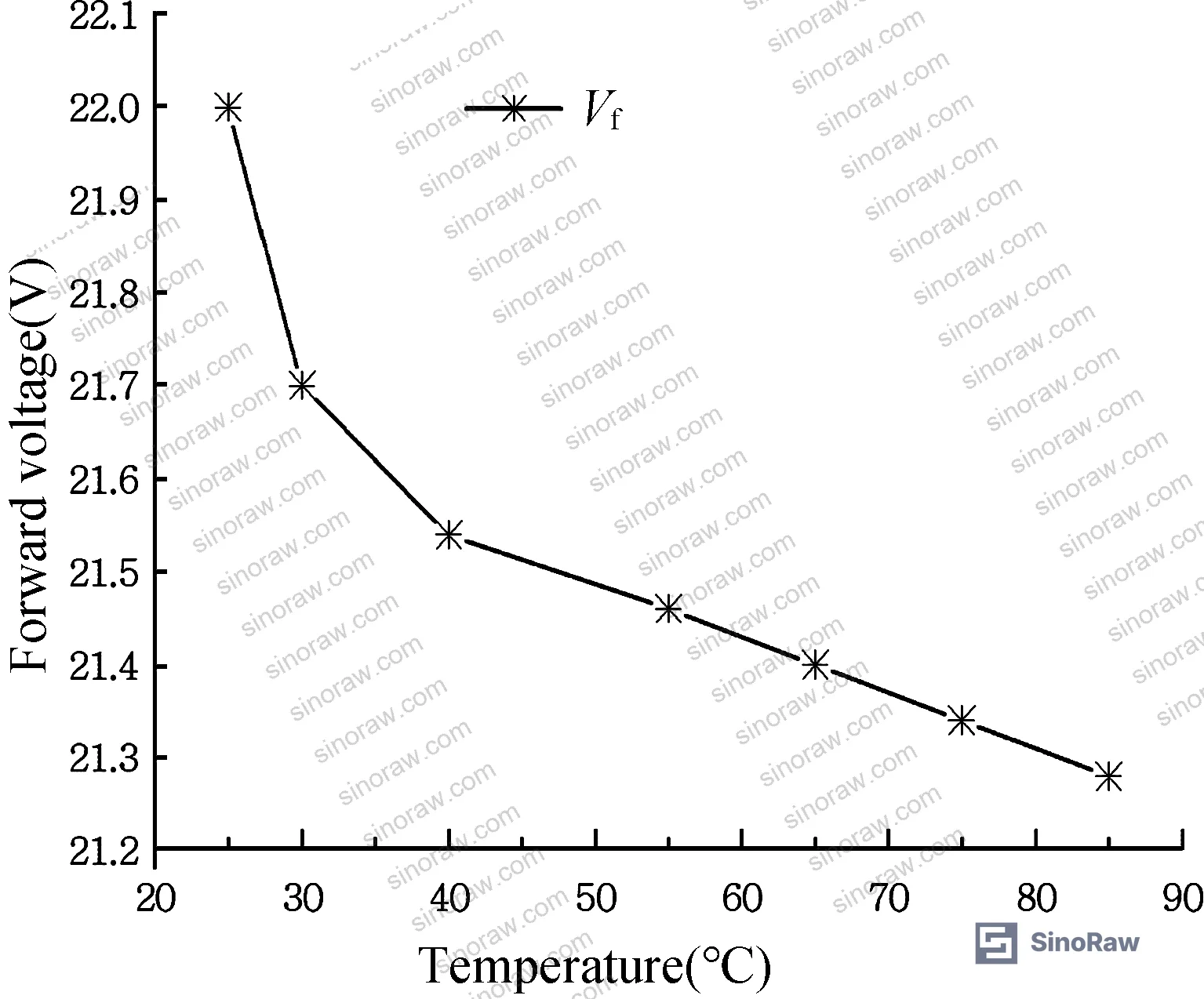
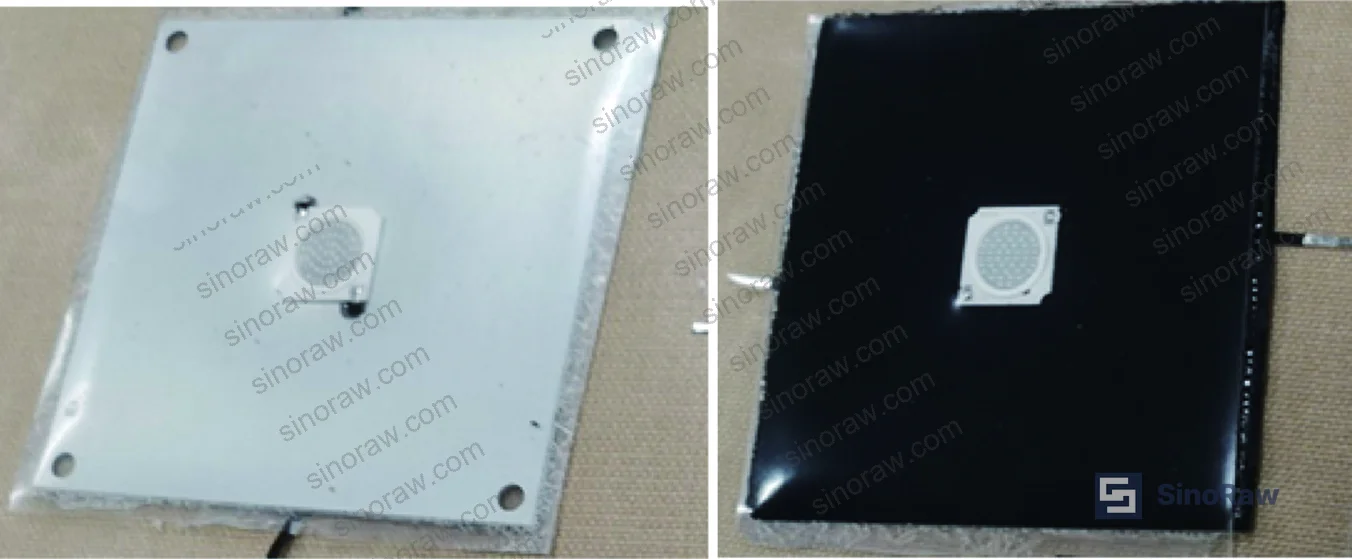
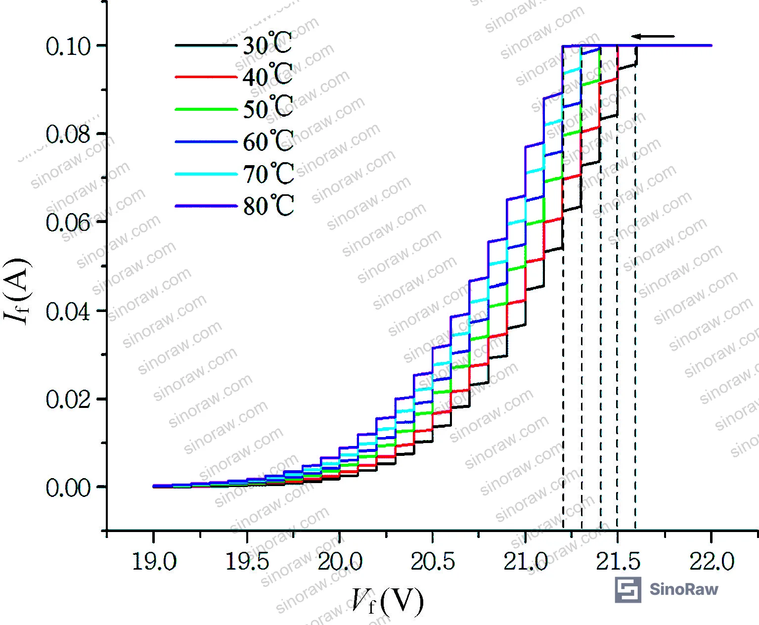
The test protocol used a 24 W COB blue-light LED source built from 48 chips in an 8-series, 6-parallel configuration, driven at 900 mA constant current in a 25 °C water bath. Junction temperature was derived from the forward voltage method, with a measured voltage temperature coefficient of −0.3 mV/K — established across the 30–80 °C characterization range. Three laminated module variants were compared head-to-head: one with no graphite layer (A1), one with a 0.03 mm graphite sheet at 1600 W/m·K horizontal conductivity (A2), and one with a 1.5 mm graphite sheet at 1200 W/m·K (A3).
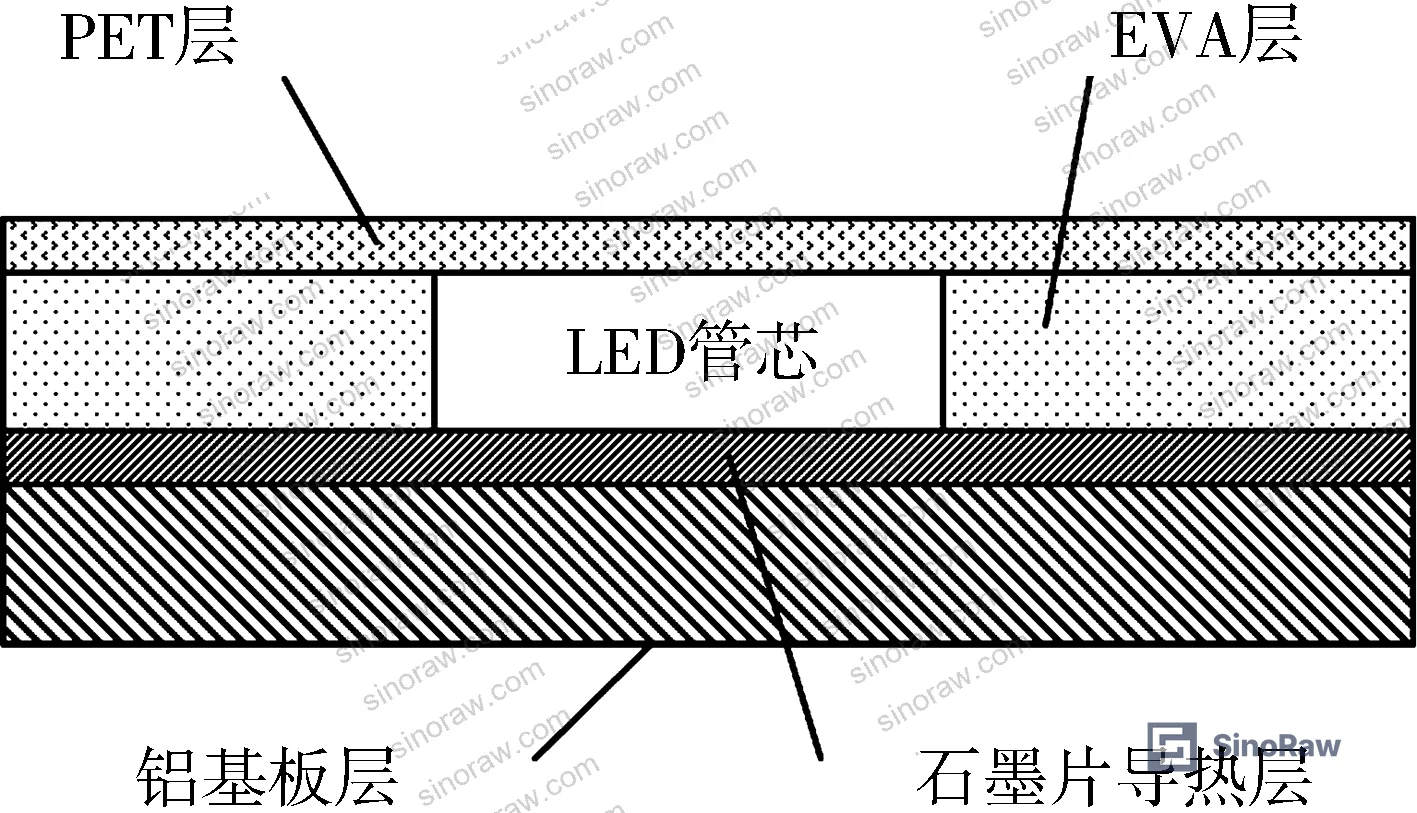
The lamination structure uses EVA (polyethylene-vinyl acetate) film as the adhesive bonding layer, PET film as the light transmission layer, and an aluminum substrate as the heat-spreading backplane — a stack architecture directly analogous to proven photovoltaic module construction, which has demonstrated field lifetimes exceeding 30 years with comparable EVA lamination systems.
Graphite Thermal Interface Layers: What the Junction Temperature Data Actually Shows #
The core finding is blunt: graphite layer horizontal thermal conductivity matters more than thickness.
Sample A1 (no graphite layer) reached a steady-state underwater junction temperature of 63.50 °C. Sample A2, using a 0.03 mm graphite sheet with horizontal conductivity of 1600 W/m·K, achieved 49.28 °C. Sample A3, using a 1.5 mm sheet with 1200 W/m·K conductivity, landed at 53.67 °C. A3 is 50 times thicker than A2 but performs worse — because the conductivity is lower.
| Sample | Graphite Thickness | Horizontal Conductivity | Junction Temp (Tj) |
|---|---|---|---|
| A1 | None (no graphite) | — | 63.50 °C |
| A2 | 0.03 mm | 1600 W/m·K | 49.28 °C |
| A3 | 1.5 mm | 1200 W/m·K | 53.67 °C |
All measurements taken at 900 mA constant current, water bath temperature 25 °C.
Honestly, most buyers over-specify graphite layer thickness when they should be specifying minimum horizontal thermal conductivity. A thicker sheet occupies more of the thermal path and, unless the conductivity is proportionally higher, simply adds resistance. The 0.03 mm / 1600 W/m·K combination is the benchmark to demand.
The forward voltage shift also confirms the thermal behavior quantitatively. Compared to A1, samples A2 and A3 showed forward voltage increases of 0.3447 V and 2.5747 V respectively under identical constant-current drive. This is thermodynamically consistent — reducing junction-to-ambient thermal resistance increases steady-state heat dissipation, which in turn raises forward voltage at fixed current. It is not a defect; it is confirmation that the thermal path is actually working.
For buyers sourcing these assemblies, this data has a direct procurement implication: ask for junction temperature test reports, not just a thermal conductivity spec sheet for the graphite material in isolation. The junction temperature under real operating conditions is what matters at end-use.
EVA Lamination Sealing: Thermal-Structural Reliability for Underwater Operation #
The lamination sealing system used in these modules deserves more attention than it typically gets in supplier qualification conversations. Interface delamination — not bulk material failure — is the primary failure mode in high-power LED assemblies. Simulation analyses of packaged LED devices show that junction temperature increases at a rate exceeding 14 °C/mm² as interfacial delamination area grows. A 4 mm² void between the chip substrate and thermal interface layer is enough to push junction temperature beyond acceptable operating limits on its own.
EVA film was selected specifically for its proven adhesion, durability, and optical transmission characteristics. The vacuum lamination process eliminates trapped air voids — the initiating defect for interfacial delamination. The technology is directly borrowed from flat-panel photovoltaic module manufacturing, where EVA-laminated assemblies routinely achieve rated field lifetimes exceeding 30 years with demonstrated resistance to temperature cycling, humidity ingress, and UV exposure.
Most procurement teams don’t realize that the IP65 rating commonly cited for commercial LED light sources does not prevent moisture vapor ingress over time — it only tests resistance to directed water jets and dust. For genuine underwater or high-humidity operation, IP65 is insufficient. A vacuum-laminated EVA structure creates a hermetically bonded stack that prevents water vapor diffusion at the material level, not just at the enclosure level. This is an important distinction when writing sourcing specifications.
Compliant suppliers operating under ISO 9001:2015 Quality management systems should be able to demonstrate documented lamination process controls — press temperature profiles, vacuum hold times, and EVA gel content post-cure — as verifiable process outputs, not just finished product inspection results.
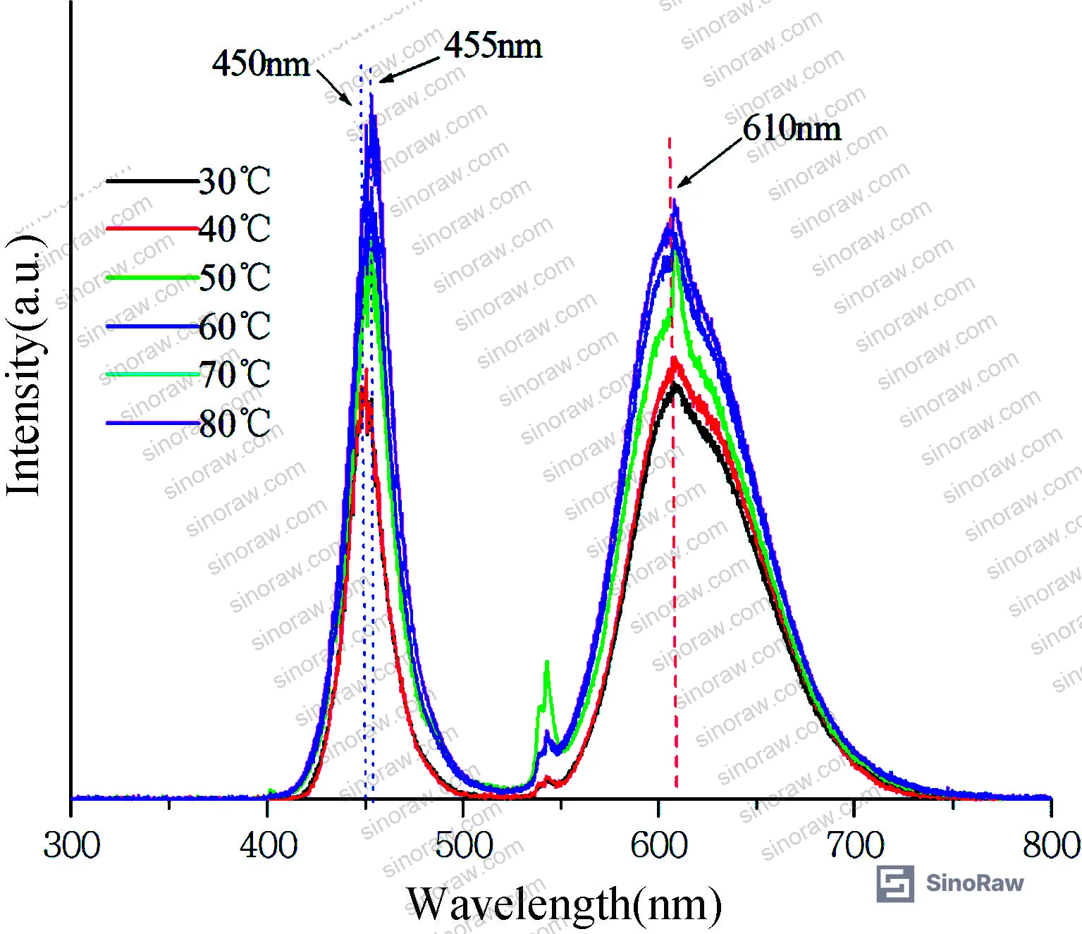
Spectral data from the red-blue COB variant (Sample B) adds another dimension to thermal qualification. Blue-chip peak emission wavelength shifted from 450 nm to 455 nm across the 30–80 °C characterization range — a 5 nm red shift consistent with bandgap narrowing in GaN-based emitters. The phosphor red peak at 610 nm showed no measurable center wavelength shift across the same temperature range. For applications where spectral stability matters — plant growth lighting, aquaculture, analytical instrumentation — managing junction temperature is directly equivalent to managing spectral output consistency.
Buyers sourcing for Sealing & Thermal applications should treat EVA gel content and lamination void rate as primary incoming inspection criteria — both are measurable, and both directly predict long-term reliability.
Practical Guidance for Buyers #
When you are qualifying suppliers for graphite-interface laminated COB LED modules, the conversation has to go beyond IP ratings and lumen specs. The data is clear: a module with no thermal interface layer operates at 63.50 °C junction temperature; the right graphite layer cuts that to 49.28 °C. That 14+ °C delta translates directly to LED lifetime — roughly halved for every 10 °C of excess junction temperature by established Arrhenius degradation models.
Request junction temperature test reports using the forward voltage method at rated drive current, not infrared surface temperature scans. Surface temperature measurements systematically underreport junction temperature and will give you false confidence. Verify the voltage temperature coefficient (should be in the −0.3 mV/K range for standard GaN blue-chip COB assemblies) — if a supplier cannot provide this calibration data, they have not done proper thermal characterization.
For the graphite TIM itself, specify minimum horizontal thermal conductivity of 1600 W/m·K rather than a minimum thickness. A 0.03 mm sheet at 1600 W/m·K outperforms a 1.5 mm sheet at 1200 W/m·K. Thick is not better.
The lamination process should use vacuum EVA bonding — not potting compound, not silicone gel filling. Verify EVA post-cure gel content (typically ≥80% by crosslink testing) and request lamination void rate data. Both are standard outputs from photovoltaic-grade lamination equipment.
At sinoraw.com, our team helps overseas procurement engineers identify and evaluate Chinese manufacturers of thermal interface materials, sealed LED modules, and related industrial components — giving you the supplier context you need before sending an RFQ. For materials covered under REACH Regulation (EC) No 1907/2006, confirm graphite purity and any adhesive additive declarations as part of your supplier qualification.
Also check the RoHS Directive 2011/65/EU compliance status for EVA film and any adhesive systems — lamination materials sourced from smaller Chinese suppliers frequently have incomplete substance declarations for these regulations.
Need help identifying qualified suppliers for graphite thermal interface layers or vacuum-laminated COB LED modules? Talk to our sourcing team →
Supplier Qualification Questions #
- What is the horizontal thermal conductivity of your graphite thermal interface layer, and can you provide test data showing values at or above 1600 W/m·K?
- Can you provide junction temperature test reports using the forward voltage method at 900 mA constant-current drive, showing Tj ≤ 50 °C in a 25 °C water bath environment?
- What is the measured voltage temperature coefficient for your COB LED assemblies — is it in the −0.3 mV/K range, and at what test current and temperature range was it characterized?
- What is the post-cure EVA gel content in your lamination process, and what vacuum profile (hold time, press temperature) do you use to achieve lamination void rates below acceptable thresholds?
- Can you provide interfacial delamination data or thermal simulation results showing junction temperature increase rate per unit delamination area — is the rate below 14 °C/mm²?
Sourcing Checklist #
- ☐ Graphite TIM horizontal thermal conductivity confirmed ≥1600 W/m·K by supplier test report, not just datasheet value
- ☐ Junction temperature under rated drive (≥900 mA) verified ≤50 °C in 25 °C ambient using forward voltage method, not IR surface scan
- ☐ Voltage temperature coefficient established at −0.3 ±0.05 mV/K range, calibrated across 30–80 °C at 100 mA test current
- ☐ EVA lamination post-cure gel content ≥80% confirmed by crosslink extraction test per photovoltaic module industry standard
- ☐ Lamination void rate documented from vacuum lamination process logs (press temperature profile, vacuum hold time, and delamination inspection record available)
- ☐ Module construction uses vacuum EVA bonding, not potting compound or silicone encapsulant
- ☐ REACH and RoHS compliance declarations available for EVA film, graphite layer, and any adhesive additives used in lamination stack
- ☐ Blue-chip peak emission wavelength red shift ≤5 nm across 30–80 °C operating range, confirmed by spectral test at rated conditions
Key Specifications Table #
| Parameter | Recommended Value | Verification Method |
|---|---|---|
| Graphite TIM horizontal thermal conductivity | ≥1600 W/m·K | Supplier test report; laser flash method preferred |
| Operating junction temperature (25 °C water bath, 900 mA) | ≤50 °C | Forward voltage method; Tj = Ta + (Vf−Va)/χ |
| LED voltage temperature coefficient | −0.3 mV/K ±10% | I-V characterization, 30–80 °C range, 100 mA test current |
| Graphite layer thickness (high-conductivity grade) | 0.03–0.05 mm | Micrometer or cross-section inspection |
| EVA gel content (post-cure) | ≥80% | Solvent extraction crosslink test |
| Blue-chip peak wavelength shift (30–80 °C) | ≤5 nm | Fiber optic spectrometer, rated drive current |
| Interfacial delamination Tj impact | <14 °C/mm² | Thermal simulation or delamination test with Tj mapping |
Can’t find a supplier meeting these specs? Submit your requirements and we’ll match you within 48 hours.
For additional context on related component categories, see our technical resources on Pneumatic Components for sealing system integration and Advanced Materials for thermal interface material selection guides.
References #
Data source: Thermal Performance of Graphite Sheet Interface Layers in Lamination-Packaged COB LED Modules for Underwater Lighting Applications, W. Yu et al., Journal of Applied Polymer Science, 2023
Frequently Asked Questions #
Why does higher thermal conductivity in the graphite layer matter more than thickness?
The thermal resistance of the interface layer depends on both thickness and conductivity — but in thin-film TIM applications, horizontal conductivity dominates because it determines how effectively heat spreads laterally before entering the aluminum substrate heatsink. Test data confirms this: a 0.03 mm sheet at 1600 W/m·K achieves lower junction temperature (49.28 °C) than a 1.5 mm sheet at 1200 W/m·K (53.67 °C), despite the second being 50 times thicker.
What is the forward voltage method for measuring junction temperature, and why is it preferred over IR imaging?
The forward voltage method derives junction temperature from the linear relationship between LED forward voltage and temperature, characterized at a known low test current (typically 1/10th of rated current — in this case 100 mA — where self-heating is negligible). Measuring the voltage shift from ambient equilibrium to operating equilibrium, divided by the voltage temperature coefficient (−0.3 mV/K), gives junction temperature directly. IR imaging only captures surface temperature, which is always lower than actual junction temperature and gives falsely optimistic readings.
Is an IP65 rating sufficient for underwater LED operation?
No. IP65 protects against directed water jets but does not prevent moisture vapor diffusion into the module over time. Vacuum EVA lamination creates a hermetically bonded stack at the material level. The same lamination technology used in photovoltaic panels has demonstrated field lifetimes exceeding 30 years with genuine moisture barrier performance — that is the standard to reference when evaluating waterproofing claims.
Why does junction temperature increase cause a spectral red shift in blue LEDs?
GaN-based blue LED chips exhibit bandgap narrowing as temperature increases, which shifts the peak emission to longer (redder) wavelengths. Across the 30–80 °C range, the tested blue chips shifted from 450 nm to 455 nm. For applications like aquaculture or plant growth lighting where spectral ratios are agronomically significant, this 5 nm shift is meaningful — and it is a direct argument for tight junction temperature control.
What drives interfacial delamination, and how does it affect module lifetime?
Thermal cycling causes differential expansion between the chip substrate, adhesive layer, and heatsink. Once a void initiates at the interface, heat can no longer transfer across that area, which raises local junction temperature — which accelerates further delamination. Analysis shows junction temperature rises at a rate exceeding 14 °C/mm² as delamination area grows. Vacuum EVA lamination eliminates the trapped air that would otherwise initiate this failure mode.
Published by sinoraw.com Technical Team | Request a sourcing quote


