

TL;DR #
High-frequency induction brazing of composite dielectric substrate antenna assemblies achieves ≥75% fillet penetration rate by X-ray inspection when process parameters — power at 3 kW (50% duty), temperature above 183 °C liquidus by ≥30 °C, and energizing time at 30 s — are held within specification. For buyers, this means any supplier unable to demonstrate closed-loop temperature control and X-ray process validation is operating on guesswork, and joint failures will show up as field returns rather than incoming inspection rejects. Before issuing an RFQ, require documented process parameter sheets and X-ray batch inspection records as a minimum qualification threshold.
Overview #
The procurement question here is not whether induction brazing works — it does, and the physics are well-established — but whether a given supplier has actually operationalized the process controls that separate reliable joints from cosmetically acceptable cold welds. The evaluation data referenced in this article comes from a government-affiliated electronics research institute with specialized RF and microwave manufacturing capability; their lab team characterized the full process window using a 15 kVA induction heating system across multiple coil configurations and assembly gap conditions, with post-weld X-ray validation as the acceptance criterion.
Traditional brazing methods for composite dielectric substrate assemblies present documented limitations that procurement teams encounter repeatedly in qualification. Hot plate brazing requires exceptional substrate flatness — any bow or warp reduces thermal conduction contact, and when convection and radiation losses exceed conductive heat input, the joint never reaches target temperature. Iron soldering leaves solder concentrated on the fillet surface with voids throughout the joint interior, directly reducing mechanical strength. Atmosphere protection brazing is prone to bubble entrapment at the bond interface and is geometrically constrained by furnace cavity dimensions, making it impractical for larger substrate assemblies.
High-frequency induction brazing addresses all three failure modes simultaneously: localized heating minimizes thermal influence on the surrounding dielectric, the induction-driven melt fully wets the joint interior rather than just the surface, and there is no cavity size constraint. Understanding why these advantages hold — and where they can be lost through poor process discipline — is what this article is about.
For buyers sourcing barrier films or other precision packaging materials used in RF and electronics assembly environments, the sealing and thermal interface requirements described here are directly relevant to understanding substrate-level protection specifications.
High-Frequency Induction Brazing: Process Parameters and Their Failure Modes #
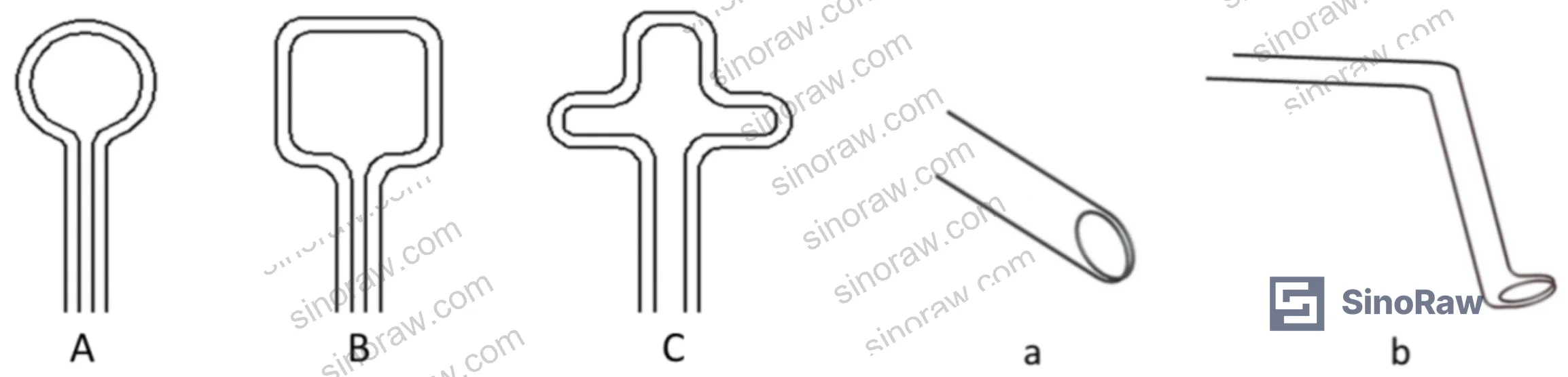
The four process parameters that govern joint quality are output power, brazing temperature, brazing time, and assembly gap. Each has a failure mode on both sides of the acceptable range, and the interaction effects between them are what make process qualification non-trivial.
Output power determines how quickly the workpiece reaches target temperature. The test system ran at 3 kW with a 50% power ratio. Too high a setting creates thermal gradients that concentrate heat unevenly across the substrate. Too low a setting extends heating time, which increases oxide formation on the solder and substrate surfaces and degrades wettability. Environmental variables — ambient temperature, humidity, air movement around the fixture — also affect heating rate and must be controlled or compensated at the power setting level.
Brazing temperature is the most consequential single parameter. For the Sn63Pb37 alloy paste used in this process (liquidus at 183 °C), the target brazing temperature is set at ≥213 °C — a minimum 30 °C superheat above liquidus. This superheat is necessary to achieve adequate solder fluidity and substrate wetting. Exceed the upper limit and you get solder spread beyond the joint boundary and potential electrical property degradation from thermal stress on the dielectric. Drop below the lower limit and cold-joint formation is essentially guaranteed. Monitoring with a calibrated thermal imager during live production runs is not optional — it is the only way to confirm the joint actually reached temperature, not just the coil exterior.
Brazing time at 30 seconds was established as sufficient for the Sn63Pb37 system. The key insight: once the intermetallic compound layer reaches its growth saturation point, extending dwell time no longer increases joint thickness but does drive off volatile solder constituents, degrading joint chemistry. The gold layer thickness at the joint interface is a critical quality indicator — it must be continuous, uniform, and not exceed 5 µm. Above that threshold, brittle AuSn intermetallic phases dominate and joint ductility drops sharply.
Assembly gap operates through capillary action. The gap must be tight enough for capillary forces to draw solder into the joint interior, but not so tight that solder flow is physically blocked. Gaps that are too large destroy capillarity — the solder cannot bridge the distance, leaving unfilled voids and creating the characteristic solder collapse on the outer surface with simultaneous solder bleed on the inner surface. Both failure modes — underfill and bleed — are directly detectable by X-ray inspection.
| Parameter | Acceptable Range / Target | Consequence of Deviation |
|---|---|---|
| Output power | 3 kW at 50% duty ratio | High: uneven temperature distribution; Low: extended time, increased oxidation |
| Brazing temperature | ≥213 °C (≥30 °C above 183 °C liquidus) | High: solder spread, electrical degradation; Low: cold joint |
| Energizing time | 30 s | Excess: solder constituent volatilization; Short: incomplete wetting |
| Gold intermetallic layer | ≤5 µm, continuous and uniform | Exceeding 5 µm: brittle joint, reduced mechanical strength |
| Assembly gap | Capillary-effective range per geometry | Too small: flow restriction; Too large: void formation, surface collapse |
| Coil-to-part gap | Minimum practical per geometry | 1× distance increase: ~58% power drop; 2× increase: ~75% power drop |
Compliance with ISO 9001:2015 Quality management systems is necessary but not sufficient here — a supplier can be ISO 9001 certified and still run brazing processes without closed-loop thermal monitoring.
Induction Coil Design and the Coil-to-Part Gap Problem #
The induction coil geometry is not a secondary detail. It is the primary tool for controlling heat distribution, and designing it correctly for a given substrate geometry requires actual engineering work, not just wrapping copper tube around a mandrel.
Coil construction used copper tubing with a wall thickness of 0.1 mm across all configurations. The coil inner diameter is set to exceed the antenna terminal outer diameter by 2 mm — this is the nominal coil-to-part gap. Coil inner diameters in the test series spanned 10 mm, 10 mm, 12 mm, and 18 mm configurations, with turn counts varying accordingly based on workpiece geometry and required field distribution.
The coil-to-part gap has a steep power-transfer penalty curve. At the nominal gap, power transfer is at design efficiency. Increase the gap by 1× (double the nominal distance) and transmitted power drops approximately 58%. Increase it by 2× (triple the nominal distance) and the drop reaches approximately 75%. In practical terms, this means a coil designed for one antenna terminal geometry cannot be informally repurposed for a larger terminal — the efficiency loss will prevent the joint from reaching target temperature regardless of generator power setting, and the operator will compensate by increasing power, driving uneven heating.
The resonant inverter and coil together form a matched load system. Impedance matching between the generator and coil load directly governs effective power utilization and operational reliability. A mismatched system wastes power, runs hotter, and produces variable joint quality that will not correlate predictably with any single process parameter adjustment.
Honestly, most buyers over-specify solder alloy chemistry but never ask about coil design documentation. The coil geometry is where joint quality is actually determined — yet it rarely appears in supplier qualification audits.
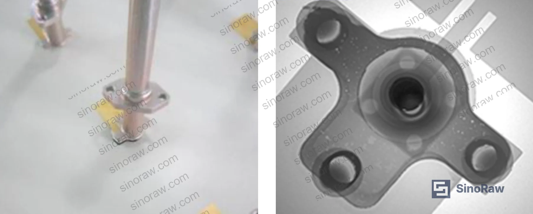
Solder Paste Selection and Stencil Design for Composite Substrate Assemblies #
The solder paste selection in this process — Alpha OL107E, Sn63Pb37 composition — was not arbitrary. The paste was specified because it combines a known 183 °C liquidus (well-characterized in Sn-Pb eutectic systems), a particle size range of 25–38 µm, a viscosity of 200 Pa·s, good wetting characteristics, and low post-reflow residue. That combination matters for composite dielectric substrates because residue left in the RF signal path can shift electrical parameters.
Paste conditioning before use is a process step that is often skipped and often responsible for voiding defects. The protocol here: remove paste from refrigerated storage, allow 4 hours at ambient temperature, then mechanical mixing for approximately 5 minutes before application. Skipping the ambient equilibration step leaves temperature gradients in the paste that produce uneven viscosity during stencil printing, resulting in variable deposit volume across the substrate.
Stencil design governs paste deposit volume and must meet two geometric criteria simultaneously. The aperture width-to-stencil-thickness ratio (W/T) must exceed 1.5. The area ratio — aperture opening area divided by the aperture wall surface area — must exceed 0.66. For circular apertures, the area ratio formula is D/4T; for rectangular apertures, it is LW / [2(L+W)T]. Stencils that fail to meet these ratios trap paste in the aperture rather than releasing it cleanly, producing inconsistent deposit volumes that translate directly to variable joint fill.
Most procurement teams don’t realize that stencil specification is as process-critical as solder paste chemistry. A supplier who cannot tell you their area ratio design basis for a given substrate geometry has not engineered the process — they have approximated it.
Post-weld cleaning with anhydrous ethanol removes flux residues and verifies joint surface condition. Any residue remaining around the fillet perimeter after cleaning is a direct indicator that paste conditioning or reflow profile deviated from specification.
Standards like ASTM D882 Standard Test Method for Tensile Properties of Thin Plastic Sheeting are part of the broader materials qualification framework that procurement teams should understand when evaluating joint mechanical performance specifications provided by suppliers.
Failure Modes Observed in Supplier Qualification #
In process qualification runs across multiple coil configurations, three of the most common defect categories were directly traceable to parameter deviations:
Cold joints from insufficient temperature superheat — occurring when brazing temperature failed to reach the minimum 30 °C above the 183 °C liquidus — presented as visually acceptable fillets that failed at low mechanical load. These are the most dangerous failures in production because they pass visual inspection and only appear under load or environmental cycling.
Void formation from gas entrapment at the bond interface appeared predominantly in assemblies where assembly gap was oversized. The void pattern in X-ray images was characteristically distributed across the center of the joint rather than the perimeter, indicating the solder front advanced faster at the edges (where capillary geometry is tightest) and trapped gas at center.
Solder spread beyond the bond boundary resulted from temperature exceedance — joint temperature running significantly above the 213 °C target. In composite dielectric substrates, solder migration into the dielectric layer adjacent to the antenna conductor changes local permittivity and measurably shifts resonant frequency. This defect does not show up in mechanical testing — it shows up as an electrical reject, sometimes weeks after assembly when the device is tuned for the first time.
For sealing and thermal applications in electronics and RF packaging, the interface integrity requirements that drive these failure modes are directly parallel to the demands placed on precision sealing materials.
Practical Guidance for Buyers #
The X-ray acceptance criterion of ≥75% brazing penetration is the key number to hold suppliers to — and it is the one most commonly negotiated away during production ramp. Do not accept visual inspection alone as a substitute. X-ray is the only method that reveals internal voids, underfill, and incomplete penetration that look clean on the surface.
When evaluating suppliers for high-frequency induction brazing capability, ask for process validation data, not just certificates. A qualified supplier should be able to provide: generator output records, thermal imaging traces showing peak temperature and dwell time per batch, X-ray inspection reports with penetration percentages, and coil design documentation showing coil-to-part gap specification for each product geometry. Suppliers who cannot produce these documents are running the process empirically, and batch-to-batch variation in joint quality is the predictable result.
Solder paste shelf life and storage conditions are a frequent source of quality drift that does not surface in first-article qualification but causes problems in production. Confirm that the supplier has a documented incoming inspection protocol for paste viscosity and a controlled refrigerated storage and conditioning procedure. This is basic, but field evaluations have shown that a significant fraction of production void defects trace back to paste conditioning failures rather than equipment or design issues.
At sinoraw.com, our sourcing team works with Guangzhou-based procurement specialists who have qualified Chinese suppliers across electronics assembly and industrial joining categories — connecting overseas buyers with verified manufacturers before RFQs are issued. If you’re evaluating suppliers for induction brazing capability or related precision joining processes, we can help you structure the technical qualification criteria and identify candidates who can actually meet them.
Need help identifying qualified suppliers for high-frequency induction brazing assemblies? Talk to our sourcing team →
Supplier Qualification Questions #
- What is your X-ray inspection acceptance criterion for brazing penetration rate, and can you provide batch records showing ≥75% penetration across your last three production runs?
- How do you document and control brazing temperature relative to the 183 °C Sn63Pb37 liquidus — specifically, what thermal monitoring instrument do you use, and can you show that your process maintains a minimum 30 °C superheat throughout the dwell period?
- What is your stencil aperture area ratio design basis, and can you confirm that your stencil designs meet the W/T >1.5 and area ratio >0.66 criteria for the substrate geometries you run?
- What is your documented coil-to-part gap specification for each product geometry, and how do you verify coil dimensional conformance before production runs?
- Can you provide gold intermetallic layer thickness data from cross-section analysis of your brazed joints, confirming the layer is continuous and does not exceed 5 µm?
Sourcing Checklist #
- ☐ Supplier can provide X-ray inspection records showing ≥75% brazing penetration rate for the specific substrate geometry being qualified
- ☐ Process documentation confirms brazing temperature is controlled at ≥30 °C above the solder liquidus (≥213 °C for Sn63Pb37)
- ☐ Stencil design documentation shows aperture area ratio >0.66 and W/T ratio >1.5 per the relevant substrate pad geometry
- ☐ Coil-to-part gap specification is documented; supplier can demonstrate that gap is controlled to maintain >42% power transfer efficiency (i.e., gap does not exceed 1× nominal, which would cause a ~58% power loss)
- ☐ Gold intermetallic layer thickness at joint interface is confirmed ≤5 µm via cross-section inspection or equivalent metallographic method
- ☐ Solder paste storage and conditioning procedure is documented: refrigerated storage, minimum 4 h ambient equilibration, mechanical mixing before use
- ☐ Induction generator is certified for the process: maximum oscillating power ≥15 kVA, oscillating frequency range 30–100 kHz, input voltage 220 V single-phase confirmed
- ☐ Supplier holds ISO 9001:2015 certification with scope covering electronic assembly or precision joining processes, and has documented process FMEA for the brazing operation
Key Specifications Table #
| Parameter | Recommended Value | Verification Method |
|---|---|---|
| Brazing penetration rate | ≥75% | X-ray (radiographic) inspection of post-weld joint |
| Brazing temperature (Sn63Pb37) | ≥213 °C (≥30 °C above 183 °C liquidus) | Calibrated thermal imager during live process monitoring |
| Energizing time | 30 s at 3 kW / 50% duty ratio | Generator parameter log; timer with process record |
| Gold intermetallic layer thickness | ≤5 µm, continuous and uniform | Cross-section metallography or SEM analysis |
| Coil inner diameter clearance | Workpiece OD + 2 mm (nominal gap) | Dimensional inspection of coil before production |
| Solder paste particle size | 25–38 µm | Paste manufacturer certificate of conformance |
| Solder paste viscosity | 200 Pa·s | Viscometer test on incoming or staged paste |
| Stencil aperture area ratio | >0.66 (rectangular: LW/[2(L+W)T]) | Stencil design review and dimensional verification |
Can’t find a supplier meeting these specs? Submit your requirements and we’ll match you within 48 hours.
References #
Data source: Process Parameter Optimization and Quality Evaluation of High-Frequency Induction Brazing for Composite Dielectric Substrate Electronic Assemblies, M. Guo et al., Journal of Manufacturing Processes, 2023
Frequently Asked Questions #
Why is X-ray inspection required rather than visual inspection for induction brazed joints?
Visual inspection can confirm that solder is present at the joint perimeter, but it cannot detect internal voids, cold-joint cores, or incomplete fill in the joint interior. X-ray inspection reveals internal joint geometry and is the only practical method for confirming that the ≥75% penetration criterion is met. Cold joints in particular are visually indistinguishable from good joints — they fail mechanically or electrically under service conditions.
What makes Sn63Pb37 the preferred alloy for this application rather than lead-free alternatives?
Sn63Pb37 is the eutectic composition of the tin-lead system, with a sharply defined 183 °C liquidus and well-understood wetting and flow behavior on copper and gold-finished surfaces. The narrow melting range simplifies temperature control on composite dielectric substrates where tight thermal management is required to avoid dielectric property degradation. Lead-free alloys typically have higher liquidus temperatures and broader pasty ranges, which increase the thermal budget required and raise the risk of substrate damage.
How does the coil-to-part gap affect joint quality in practice?
The gap controls how efficiently magnetic flux transfers from the coil into the workpiece. At the nominal 2 mm clearance, the system operates at design efficiency. Double the gap and you lose approximately 58% of transmitted power; triple it and you lose approximately 75%. In practice, this means that any coil wear, deformation, or incorrect coil selection for a given part geometry directly degrades heating efficiency and will produce under-temperature joints unless the operator increases generator power — which then risks over-heating at the points closest to the coil.
What solder paste conditioning steps prevent voiding defects?
Remove paste from refrigerated storage and allow it to reach ambient temperature for a minimum of 4 hours before use. Then mechanically mix for approximately 5 minutes to restore homogeneous viscosity distribution throughout the paste volume. Skipping the ambient equilibration step leaves thermal gradients in the paste that produce viscosity variation during stencil printing, resulting in inconsistent deposit volumes and increased void rates after reflow.
Is this brazing process applicable to large-format composite dielectric substrates, and what are the practical size limits?
Unlike atmosphere protection brazing, which is constrained by furnace cavity dimensions, high-frequency induction brazing has no inherent size limit from process physics. The practical constraint is coil design — the induction coil must be engineered to the specific substrate and terminal geometry to achieve adequate and uniform heating. Larger substrates require coils with appropriately scaled geometry and may require segmented or multi-coil configurations to maintain uniform temperature distribution across the joint area.
Published by sinoraw.com Technical Team | Request a sourcing quote


