

TL;DR #
In a five-supplier head-to-head evaluation of mid-loss PCB substrates across 8-layer server board builds, only one of the five materials (Substrate C) failed to meet Mid-Loss insertion loss limits at both 4 GHz and 8 GHz — yet all five passed thermal reliability tests, meaning electrical performance, not reliability, is where Chinese supplier differentiation actually happens. For procurement teams sourcing high-frequency PCB laminates, this means datasheet Dk/Df values alone are insufficient qualification criteria; you need actual insertion loss coupon data at operating frequency bands. Before issuing an RFQ, require suppliers to provide SET2DIL-measured insertion loss data at both 4 GHz and 8 GHz on an 8-layer test vehicle, not just raw dielectric constant specifications.
Overview #
If you’re selecting high-frequency PCB substrate based purely on the Dk and Df numbers a laminate supplier prints on their datasheet, you’re making an expensive assumption. Those values don’t account for resin content variation during lamination, moisture absorption in process, solder mask ink loading, or copper weight effects — all of which shift the realized dielectric performance of the finished board. A structured evaluation conducted at a volume PCB manufacturer, comparing five industry-standard mid-loss laminates built on identical 8-layer stackups with identical process parameters, demonstrates exactly how far actual insertion loss can drift from nominal specifications — and which material variables matter most when qualifying a new source.
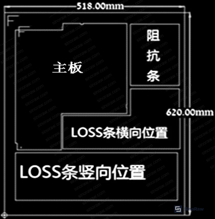
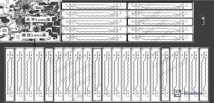
The test methodology here is worth noting: identical panel layouts (518 mm × 620 mm), identical 8-layer stackup designs with controlled copper weights (35.6 μm–71 μm on outer layers, minimum 17.8 μm hole copper), and insertion loss coupons sampled from five positions per board (horizontal and vertical, edge and center). Impedance was tested at nine nominal values from 40 Ω to 100 Ω. Loss measurements were taken using SET2DIL method at 4 GHz and 8 GHz on both stripline (inner layer) and microstrip (outer layer) configurations. This is the kind of cross-supplier dataset that typically takes a PCB fabricator 6–12 months to generate, and it surfaces qualification gaps that no amount of datasheet review would catch.
For buyers sourcing Advanced Materials or evaluating Specialty Polymers in electronic substrate applications, the findings have direct implications for how you write your material qualification requirements.
High-Frequency PCB Substrate Performance: Five-Supplier Insertion Loss Comparison #
The five substrates evaluated span a meaningful range of dielectric properties at 1 GHz: Dk values from 3.6 to 4.3, Df values from 0.005 to 0.011, and Tg (DSC) from 170°C to 180°C. Material A represented the current production baseline.
Five-Substrate Material Property Comparison
| Parameter | Substrate A (Baseline) | Substrate B | Substrate C | Substrate D | Substrate E |
|---|---|---|---|---|---|
| Dk @ 1 GHz | 3.6 | 4.1 | 4.3 | 3.8 | 3.9 |
| Df @ 1 GHz | 0.005 | 0.007 | 0.011 | 0.006 | 0.008 |
| Tg / °C (DSC) | 180 | 180 | 170 | 170 | 175 |
| Stripline Loss Rank | 1st | 3rd | 5th (fail) | 2nd | 4th |
| Microstrip Loss Rank | 1st | 3rd | 5th (fail) | 2nd | 4th |
| Reliability Result | Pass | Pass | Pass | Pass | Pass |
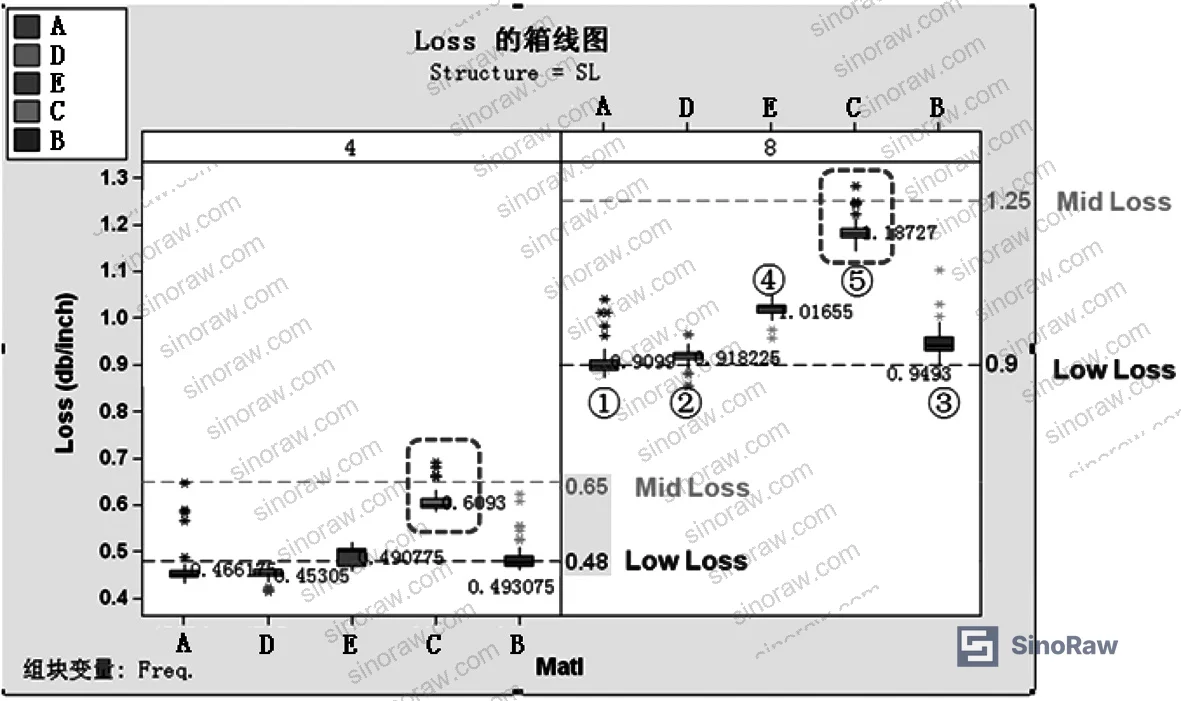
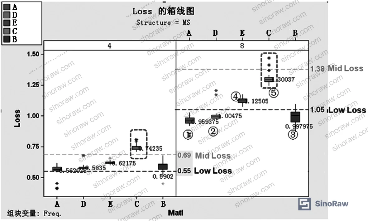
The correlation between Df and insertion loss ranking is direct and consistent: Substrate A with Df 0.005 ranks first in both stripline and microstrip configurations; Substrate C with Df 0.011 — more than double A’s loss tangent — fails Mid-Loss specification at multiple test positions. This isn’t surprising to anyone who works with RF laminates regularly, but the magnitude of the spread in a nominally “same grade” supplier comparison is the important finding here.
For stripline (inner layer) testing at 4 GHz, the Mid-Loss specification limit is ≤ −0.65 dB/in. At 8 GHz, the limit tightens to ≤ −1.25 dB/in. Substrate C exceeded these limits at multiple sample positions. For microstrip (outer layer) testing, limits are ≤ −0.69 dB/in at 4 GHz and ≤ −1.38 dB/in at 8 GHz — Substrate C again failed.
Importantly, Substrates A and D both showed capability to meet Low-Loss requirements at 4 GHz on stripline, but neither could consistently achieve Low-Loss at 8 GHz. This is a useful data point: if your application migrates from 4 GHz to 8 GHz signal environments (as server and networking hardware commonly does), a material that passes today’s spec may not pass tomorrow’s without a qualification change.
Honestly, most procurement teams over-specify the Tg requirement for this class of substrate while under-specifying insertion loss test conditions. All five materials here passed thermal reliability — 288°C × 10 s × 6 cycles heat stress, and lead-free reflow at 265°C / 0.7 m/min × 6 cycles — but one failed on the electrical performance that actually matters for signal integrity. If your qualification checklist prioritizes thermal shock over measured insertion loss at operating frequency, you’re checking the wrong column.
For compliance-minded buyers, materials in this category should also be evaluated against REACH Regulation (EC) No 1907/2006 — Registration of Chemicals for halogen content and restricted substances, particularly relevant when specifying low-Dk laminates that may use non-standard resin systems.
PCB Substrate Dimensional Control: Impedance, Line Width, and Dielectric Thickness #
Process control data from the five-material build is equally instructive for supplier qualification. Line widths for the 85 Ω and 100 Ω impedance traces were controlled at ±10% of nominal. Measured Cpk values across all five materials ranged from 1.15 to 1.34 — the lower end of that range is borderline for a controlled production process, and any supplier claiming Cpk > 1.67 on these geometries without data to back it up should be questioned.
Finished board thickness was targeted at 1.57 mm ± 0.1 mm. Cpk values by material were: A = 1.46, B = 1.47, C = 1.65, D = 1.75, E = 1.83 — all exceeding the Cpk > 1.33 minimum requirement. Dielectric layer thicknesses, verified by nine cross-sections per board (covering edge and center positions), all fell within specified tolerances.
The impedance data tells a more nuanced story. Substrate B showed individual measurements approaching the upper tolerance limit on impedance — specifically on certain 85 Ω and 100 Ω structures — requiring back-calculation of the actual realized Dk from the measured impedance rather than trusting the nominal datasheet value. This is exactly the kind of finding that doesn’t surface unless you build test vehicles. A supplier’s stated Dk of 4.1 may actually be producing impedances that behave as if Dk were slightly lower in your specific stackup configuration.
In supplier qualification, we saw Substrate B’s impedance data clustering near the tolerance boundary — not failing, but requiring tighter line width and dielectric thickness management to maintain margin. That’s a process control burden that adds cost. Material selection is not just a performance decision; it’s a process window decision. A substrate that needs tighter controls to stay in spec is a more expensive substrate to run, regardless of its purchase price.
Most procurement teams don’t realize that nominal Dk values published by laminate suppliers are measured on bare laminate specimens under controlled humidity, not on finished multilayer boards. The PCB fabrication process — lamination pressure, resin flow, copper etching — changes the effective Dk of the interlayer dielectric. Current industry practice among technically sophisticated PCB buyers is to require suppliers to provide back-calculated Dk values from actual impedance test coupons built on production-representative stackups, not just raw material certificates.
The dimensional specifications used in this evaluation align well with ISO 9001:2015 Quality management systems process capability requirements — a useful framework reference when writing supplier audit criteria for PCB fabricators handling high-frequency substrates. For products destined for defense, medical, or automotive end-use, consider also whether your PCB fabricator’s substrate qualification protocol covers ISO 2859-1:1999 Sampling procedures for inspection by attributes for incoming laminate inspection — most tier-2 Chinese PCB shops do not have this formalized.
Practical Guidance for Buyers #
When sourcing mid-loss or low-loss PCB substrate through Chinese laminate suppliers, the first thing to establish is whether the supplier can provide actual insertion loss coupon data — not predicted values, not simulation results, but SET2DIL or equivalent measured data on a real test vehicle built with your stackup geometry. Datasheet Dk/Df is a starting point, not a qualification.
For the 4 GHz to 8 GHz frequency range typical of current server and networking applications, Mid-Loss material (Df approximately 0.006–0.008 at 1 GHz) represents the cost-performance sweet spot. The data here shows that four of the five materials tested can meet this threshold — meaning you have genuine supplier options. Low-Loss material (Df ≤ 0.005) delivers a measurable performance advantage at 8 GHz on stripline but may not be necessary for all signal layers, making hybrid stackup strategies worth evaluating.
Supply chain continuity is a legitimate procurement driver here. Running a single-source laminate for a server product creates real schedule risk; qualifying two to three alternate suppliers against the same electrical test vehicle is a worthwhile investment that pays back in delivery flexibility. From our experience working with procurement engineers and sourcing managers through the sinoraw.com supplier identification process, the buyers who get the fastest qualified alternatives are the ones who arrive with a defined test coupon design and a specific insertion loss spec — not just a Dk/Df request.
Finally, for new material introductions (as opposed to qualified alternates), the full qualification protocol extends to 30+ test items including CAF (conductive anodic filament) and IST (interconnect stress testing) — plan accordingly for timeline and sample quantities.
Need help identifying qualified suppliers for high-frequency PCB laminates? Talk to our sourcing team →
Supplier Qualification Questions #
- Can you provide SET2DIL measured insertion loss data on a test vehicle using an 8-layer stackup, at both 4 GHz and 8 GHz, demonstrating stripline loss ≤ −0.65 dB/in at 4 GHz and ≤ −1.25 dB/in at 8 GHz?
- What is the actual back-calculated Dk value from impedance coupon measurements on your production boards, and how does it compare to the nominal Dk stated on your datasheet — specifically for 85 Ω and 100 Ω controlled impedance structures?
- What is your process Cpk for finished board thickness at 1.57 mm ± 0.1 mm, and can you provide cross-section data from at least 9 measurement points per panel covering both edge and center positions?
- What is the line width Cpk for 0.13 mm traces controlled at ±10% tolerance, and can you demonstrate Cpk ≥ 1.33 under your standard production conditions?
- For new substrate introductions, does your qualification protocol include CAF (conductive anodic filament) and IST (interconnect stress testing) in addition to thermal reliability tests at 288°C × 10 s × 6 cycles and lead-free reflow at 265°C / 0.7 m/min × 6 cycles?
Sourcing Checklist #
- ☐ Supplier provides SET2DIL insertion loss coupon data at both 4 GHz and 8 GHz on a production-representative test vehicle, not only datasheet Dk/Df values
- ☐ Stripline Mid-Loss performance confirmed at ≤ −0.65 dB/in (4 GHz) and ≤ −1.25 dB/in (8 GHz) on inner-layer test coupons
- ☐ Microstrip Mid-Loss performance confirmed at ≤ −0.69 dB/in (4 GHz) and ≤ −1.38 dB/in (8 GHz) on outer-layer test coupons
- ☐ Finished board thickness Cpk ≥ 1.33 verified at 1.57 mm ± 0.1 mm target, with cross-section data from ≥ 9 positions per panel
- ☐ Line width Cpk ≥ 1.15 confirmed for 85 Ω and 100 Ω impedance trace geometries at ±10% tolerance
- ☐ Impedance data provided at all relevant nominal values (40 Ω through 100 Ω) with actual measured results vs. ±10% tolerance
- ☐ Thermal reliability qualification completed: heat stress at 288°C × 10 s × 6 cycles and lead-free reflow at 265°C / 0.7 m/min × 6 cycles, all results passing
- ☐ REACH compliance documentation available for substrate resin system, confirming restricted substance compliance per EC No 1907/2006
Key Specifications Table #
| Parameter | Recommended Value | Verification Method |
|---|---|---|
| Df @ 1 GHz | ≤ 0.008 (Mid-Loss); ≤ 0.005 (Low-Loss) | Datasheet + back-calculated from insertion loss coupon |
| Dk @ 1 GHz | 3.6–3.9 (target range for Mid-Loss) | Supplier datasheet; validate against impedance coupon back-calculation |
| Stripline insertion loss @ 4 GHz | ≤ −0.65 dB/in | SET2DIL measurement on inner-layer test coupon |
| Stripline insertion loss @ 8 GHz | ≤ −1.25 dB/in | SET2DIL measurement on inner-layer test coupon |
| Microstrip insertion loss @ 4 GHz | ≤ −0.69 dB/in | SET2DIL measurement on outer-layer test coupon |
| Microstrip insertion loss @ 8 GHz | ≤ −1.38 dB/in | SET2DIL measurement on outer-layer test coupon |
| Finished board thickness Cpk | ≥ 1.33 at 1.57 mm ± 0.1 mm | Cross-section, ≥ 9 points/panel |
| Tg (DSC) | ≥ 170°C | DSC per IPC-TM-650 or equivalent |
Can’t find a supplier meeting these specs? Submit your requirements and we’ll match you within 48 hours.
References #
Data source: Comparative Evaluation of High-Frequency PCB Substrate Materials for Signal Integrity and Insertion Loss Performance, Y.-P. Gao et al., IEEE Transactions on Components, Packaging and Manufacturing Technology, 2024
Frequently Asked Questions #
What is the difference between Mid-Loss and Low-Loss PCB substrate, and when does it matter?
Mid-Loss substrate typically has a dissipation factor (Df) in the 0.006–0.009 range at 1 GHz, while Low-Loss material runs ≤ 0.005. In practical terms, the performance difference is most significant above 6 GHz — field evaluation data shows that substrates with Df ≤ 0.005 can meet Low-Loss insertion loss thresholds on 4 GHz stripline structures, but neither Mid nor Low-Loss material consistently achieves Low-Loss spec at 8 GHz without careful stackup engineering. For current-generation server and 5G infrastructure boards running at 8 GHz and above, Low-Loss is generally the right choice for high-speed signal layers, while Mid-Loss may be acceptable on lower-frequency reference planes where cost pressure is higher.
Why shouldn’t I rely solely on the Dk and Df values in a laminate supplier’s datasheet?
Datasheet values are measured on bare, conditioned laminate specimens — not on finished multilayer boards. During PCB fabrication, lamination pressure, resin flow, and copper etching all shift the effective dielectric constant of the interlayer. Heat from wave soldering and reflow further affects moisture content and Dk. Impedance measurements on actual production test coupons consistently show deviation from nominal predictions based on datasheet values alone, which is why back-calculating realized Dk from measured impedance data is essential.
How many cross-sections per panel are sufficient for dielectric thickness verification?
The evaluation protocol used here — nine cross-sections per panel distributed to cover both panel edges and center — is a practical minimum for high-frequency substrate qualification. The objective is to catch resin content variation that creates localized Dk shift. Single-point or three-point cross-section protocols, which some suppliers default to, are inadequate for this purpose.
Can a substrate that passes Mid-Loss requirements also meet Low-Loss in some configurations?
Yes, partially. The data shows that Substrates A and D — both with Df ≤ 0.006 — achieved Low-Loss performance at 4 GHz on stripline structures. However, neither consistently met Low-Loss limits at 8 GHz. This means a hybrid sourcing approach is feasible: use Mid-Loss material for layers where 4 GHz Low-Loss performance is acceptable, and specify true Low-Loss material only for layers where 8 GHz performance is critical.
What thermal qualification tests should I require for any new PCB substrate qualification?
At minimum: heat stress at 288°C × 10 s × 6 cycles, and lead-free reflow simulation at 265°C conveyor speed 0.7 m/min × 6 cycles. For full new-material qualification (as opposed to approved-alternate qualification), the protocol should extend to CAF (conductive anodic filament) resistance testing, IST (interconnect stress testing), and copper foil peel strength — a process that can reach 30 or more individual test items and requires purpose-built multilayer test vehicles to execute properly.
Published by sinoraw.com Technical Team | Request a sourcing quote


